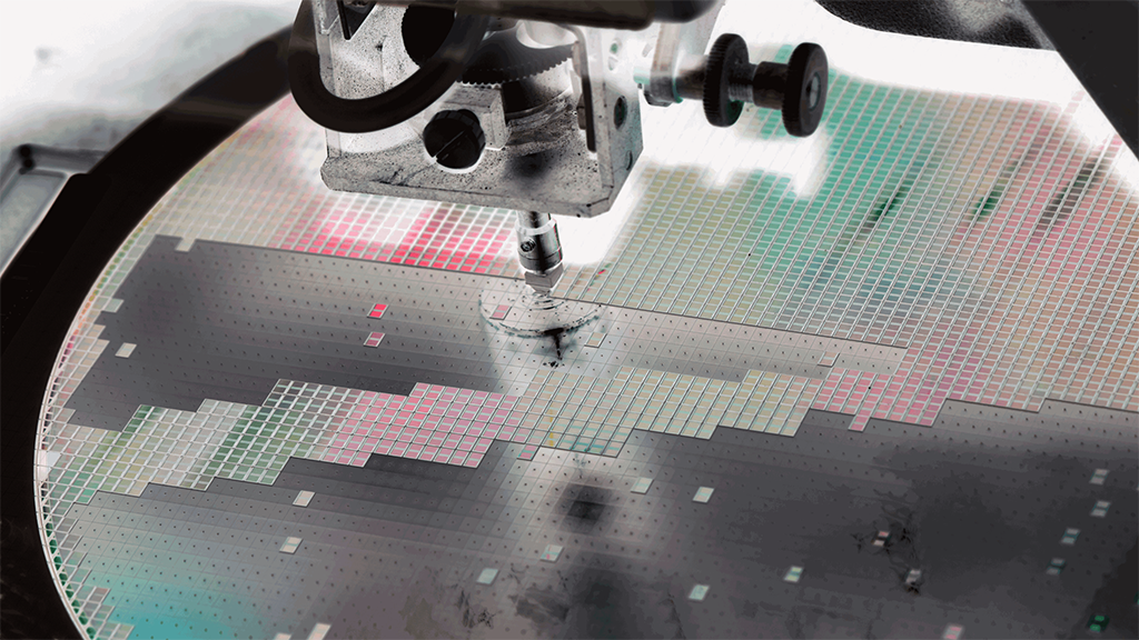
Ocean Insight partnered with a leading innovator in plasma-etching technologies, to explore full-spectrum plasma monitoring solutions suitable for detecting critical wafer etch endpoints
With the rapidly increasing global demand for semiconductors, the industry is well-positioned to invest in cost-saving process improvements and the development of increasingly sophisticated semiconductor designs and recipes. To feed today’s technology boom and weather the expanding market, semiconductor foundries require quantitative, accurate and high-speed process measurements.
Semiconductors and microelectromechanical systems (MEMS) are reaching design limitations, where further improvement via size reduction or increased speed is nearly impossible. Instead, manufacturers are focusing on wafer quality, repeatability and overall yield, as well as increased production capacity. The goal is to meet the growing demand for smart electronics while maintaining production costs and keeping prices competitive.